Design and Justification
The buck-boost circuit that was used during the alpha prototype was the most simplistic topology involving just one-switch in the buck-boost converter. Based on a published paper by the Department of Electrical and Electronics Engineering SSN College of Engineering [1], the one switch steps up/steps down the converter that we uses has a relatively high voltage and current stress on components overtime compare to the buck or boost converter. By using different topologies with more than 1 transistor, the efficiency of the converter could be significantly increased to over 90%. Oculus has chose a new 4-switches mode selection buck-boost converter (figure 1).
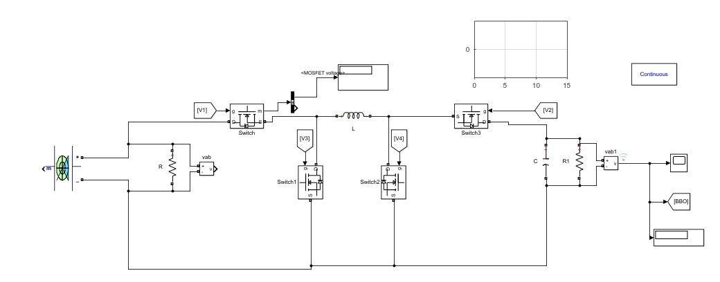
Figure 1. 4 switches buck boost converter
Due to having 3 extra transistors, the circuit requires a more complicated controller compare to the previous design. The circuit operates on 3 different modes with 4 different switching states (Figure 2).
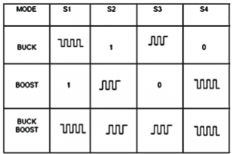 Figure 2. Switching states of the Buck boost converter
Oculus has developed a controller that could be used to control the circuit. The mode selection circuit is a state machine that would detect the output voltage, and decide which operation mode the circuit will run on by comparing it with the reference voltage (22.5V).
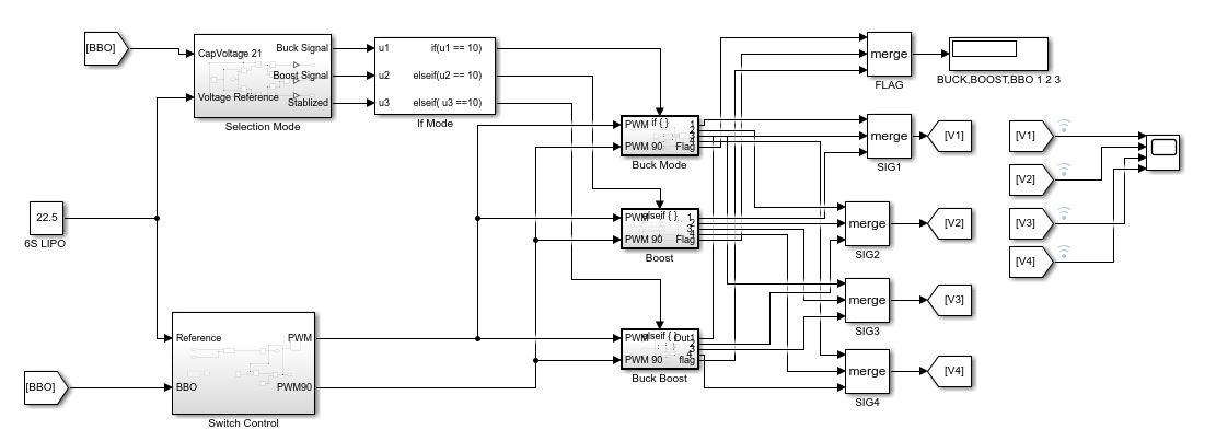 Figure 3. The control system
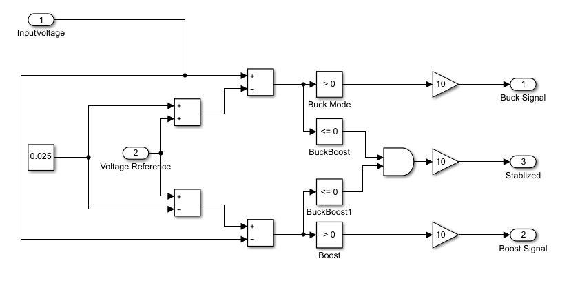 Figure 4. Selection mode
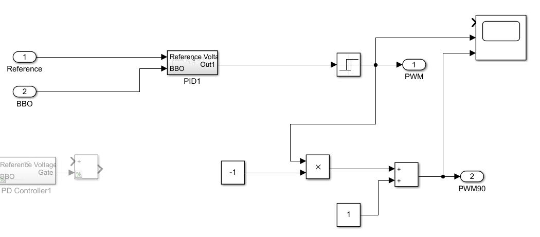
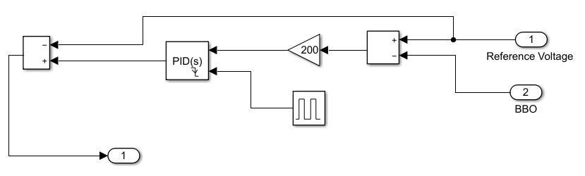
Figure 5 & 6. PID control
Result
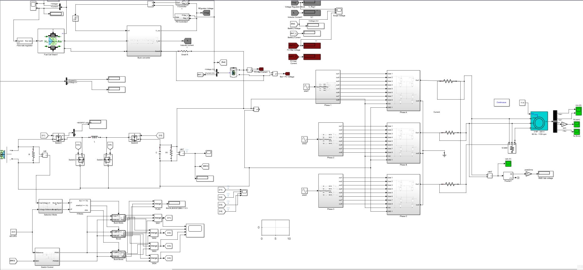
The new design buck-boost converter has shown a lot of promising results, between the first submission on March 1st to current date, Oculus has managed to have some significant progress. The problem with the control circuit earlier has been fixed and now it’s working and capable of producing clear signals (figure 7).
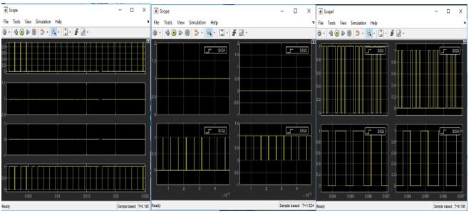
Figure 7. Buck mode, boost mode, and buck-boost mode control signals
The reference voltage was set to be at 22.5V (typical voltage for 6s battery system). Although the circuit itself has yet to be able to produce a clean and reliable waveform, it indicates the circuit work exactly how it was designed to be (figure 8). Based on the reading, the most logical reason for such signal has to be from out of tune PID control. Oculus believe once the PID has been tune up to match the circuit, the signal should be clean up and a stable output voltage will be produced
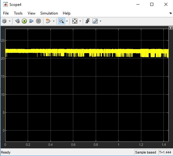
Figure 8. Output signal.
Figure 9 shows our model for the entire power system of the drone
UPDATE: Saturday Mar 16, 2019 . 4:08pm
Based on the signals (figure below), I have pinpoint where the bug might be. For some unknown reason, the PID control stopped working during the boost mode. I have some suspicious why this is happening and have a plan to tackle this. Right now I’m using 1 PID for everything, there is a possibility I have to build a dedicated control for each mode. Before I do anything, I would need to go back to my drawing board and recheck my TF calculations.
UPDATE: Monday Mar 18, 2019 . 10:14pm
A PID control was replaced by a PI control. I rechecked my math (figure 11) and was able to determine the correct duty cycle and managed to clean up the signal noise. However I have yet to determine the cause of the bug shown in 2 figures below. I have determined it must be within the PI control itself
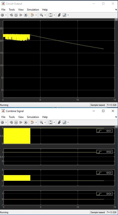
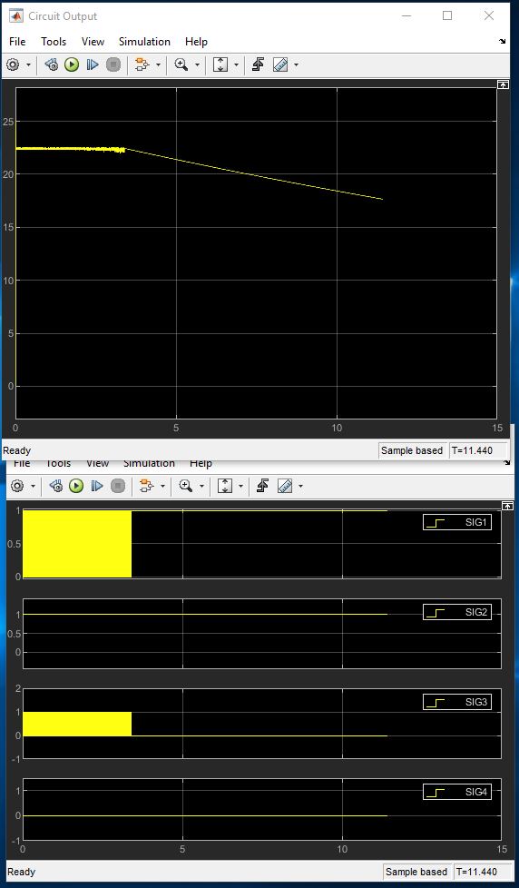
Figure 10a. Output signal on 3/16/19 & 3/18/19

Figure 11. Circuit analysis
UPDATE: Monday Mar 26, 2019 . 1:03 am:
One week has passed since the last update, the main culprit has been finally identified. After recheck and confirm my math and logic, it has been clear to me the problem must lie with Simulink itself. Having a PID control within multiple blocks has proved to be hard for Simulink to process, and thus fail to produce the intended signals. After multiple different design configurations, I have nailed down the one that would work with my model. Figure 12 below shows the control signals as intended and figure 13 shows the voltage output
Figure 12. Control signals
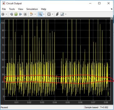
Figure 13. Output signal
Despite having a lot of noise and being very unstable, the signal has indicated that the output voltage hovers around 22.5V (Reference voltage). There are still a lot of work ahead to clear up the signal, but so far the output voltage looks very promising
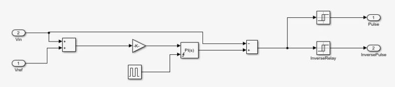
Figure 14. New PI controller